

Semiconductor Solutions
Polishing Ver 1.8
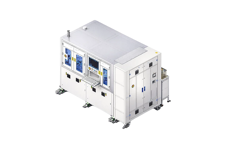
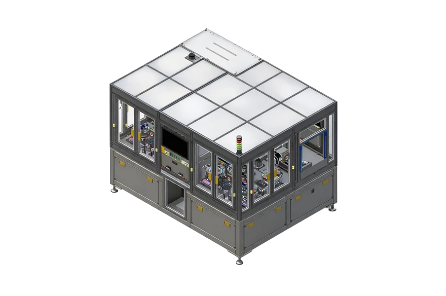
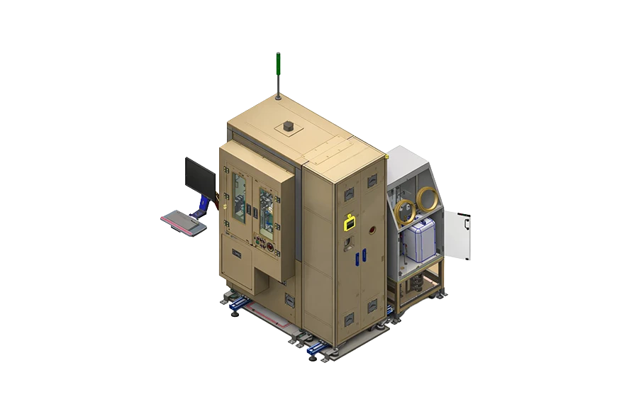
SPAS pre-treatment equipment that interfaces with the machine to automatically polish and clean molded specimens loaded by operators.
SEMICONDUCTOR SOLUTIONS
Polishing Ver 1.8
SPECIFICATION
-
Dimensions1,505(L) x 720(W) x 2,100(H)
-
WeightApprox 1,500kg
-
AP FieldSemiconductor
-
WaferMax. 20(W) x 20(D)
-
Polish JigØ30 x 5(T) / Ø48 x 7(T)
FEATURES
Applies a load of 1 to 10 N to the specimen during polishing, then rinses and cleans it using DI water while simultaneously spinning at 3,000 rpm for drying.