

Semiconductor Solutions
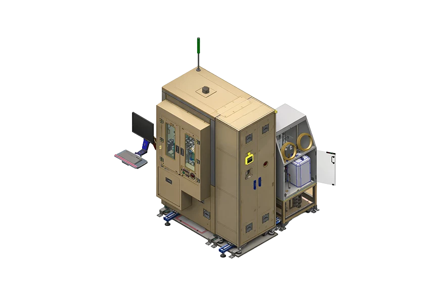
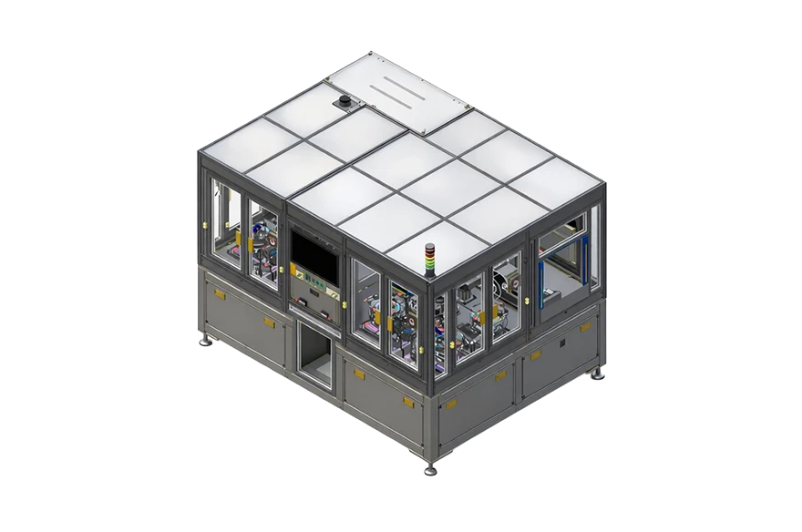
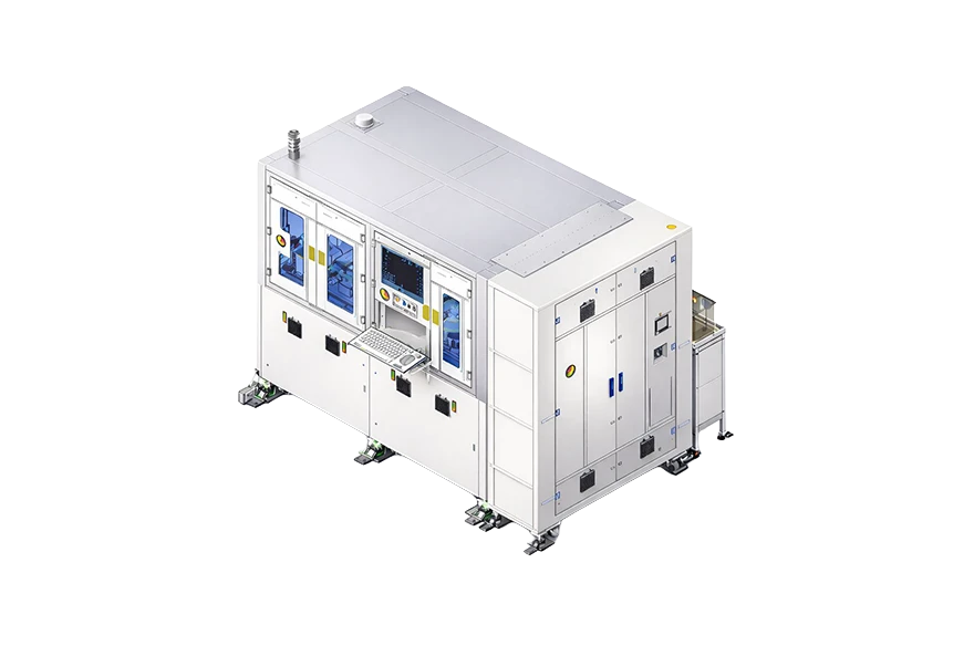
Polishing Ver 3.0
Equipment that automatically loads wafer specimens from stubs supplied by AMR robots, tilts the specimens from a vertical position for polishing and cleaning, and automatically unloads them.
SEMICONDUCTOR SOLUTIONS
Polishing Ver 3.0
SPECIFICATION
-
Dimensions2,815(L) x 1,530(W) x 2,000(H)
-
WeightApprox 6,500kg
-
AP FieldSemiconductor
-
Wafer10(L) x 10(W) x 0.8(T)
-
Polish Jig75(D) x 75(W) x 8.5(T)
FEATURES
Designed to grip specimens horizontally by vacuum suction and polish their edges at an angle of 3° to 5°.