

Semiconductor Solutions
Polishing Ver 4.0
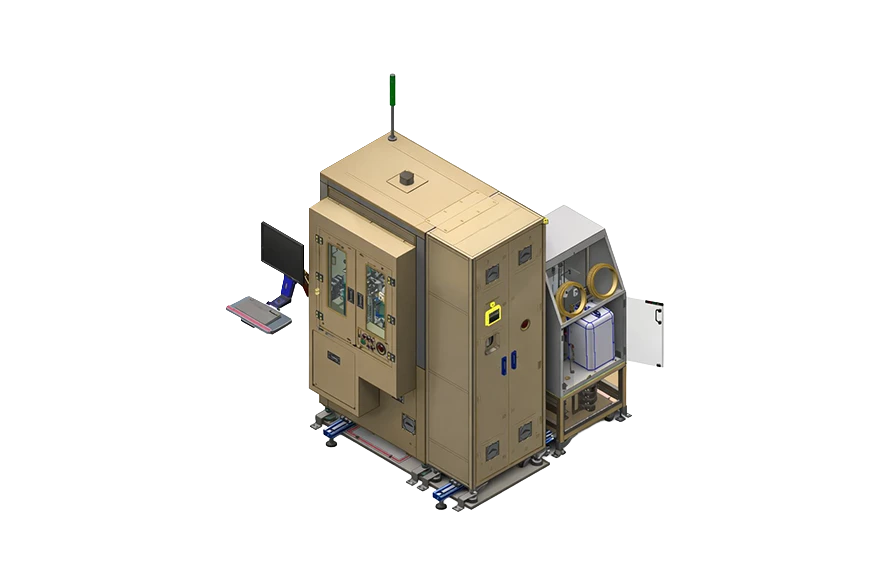
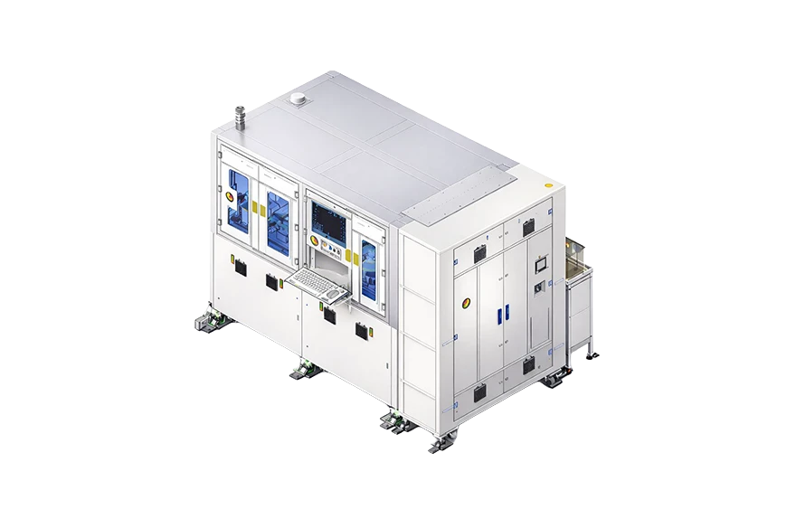
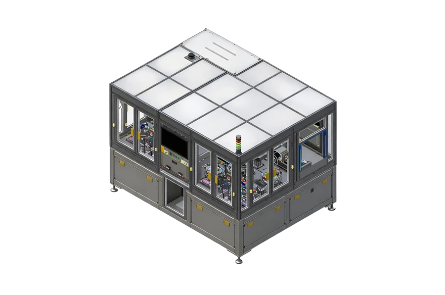
Equipment that automatically loads wafer specimens from stubs supplied by AMR robots, tilts the edges of the specimens from a vertical position for polishing and cleaning, and automatically unloads them.
SEMICONDUCTOR SOLUTIONS
Polishing Ver 4.0
SPECIFICATION
-
Dimensions2,800(L) x 2,100(W) x 2,000(H)
-
WeightApprox 3,500kg
-
AP FieldSemiconductor
-
Wafer57(L) x 35.6(W) x 12.5(H)
-
Polish Jig7(D) x 7(W) x 0.78(T)
FEATURES
Tilts the specimens by no more than 0.1° within a 5 mm range and polishes their edges, processing up to six specimens per cycle.